Codesign the material and the process that makes it real.
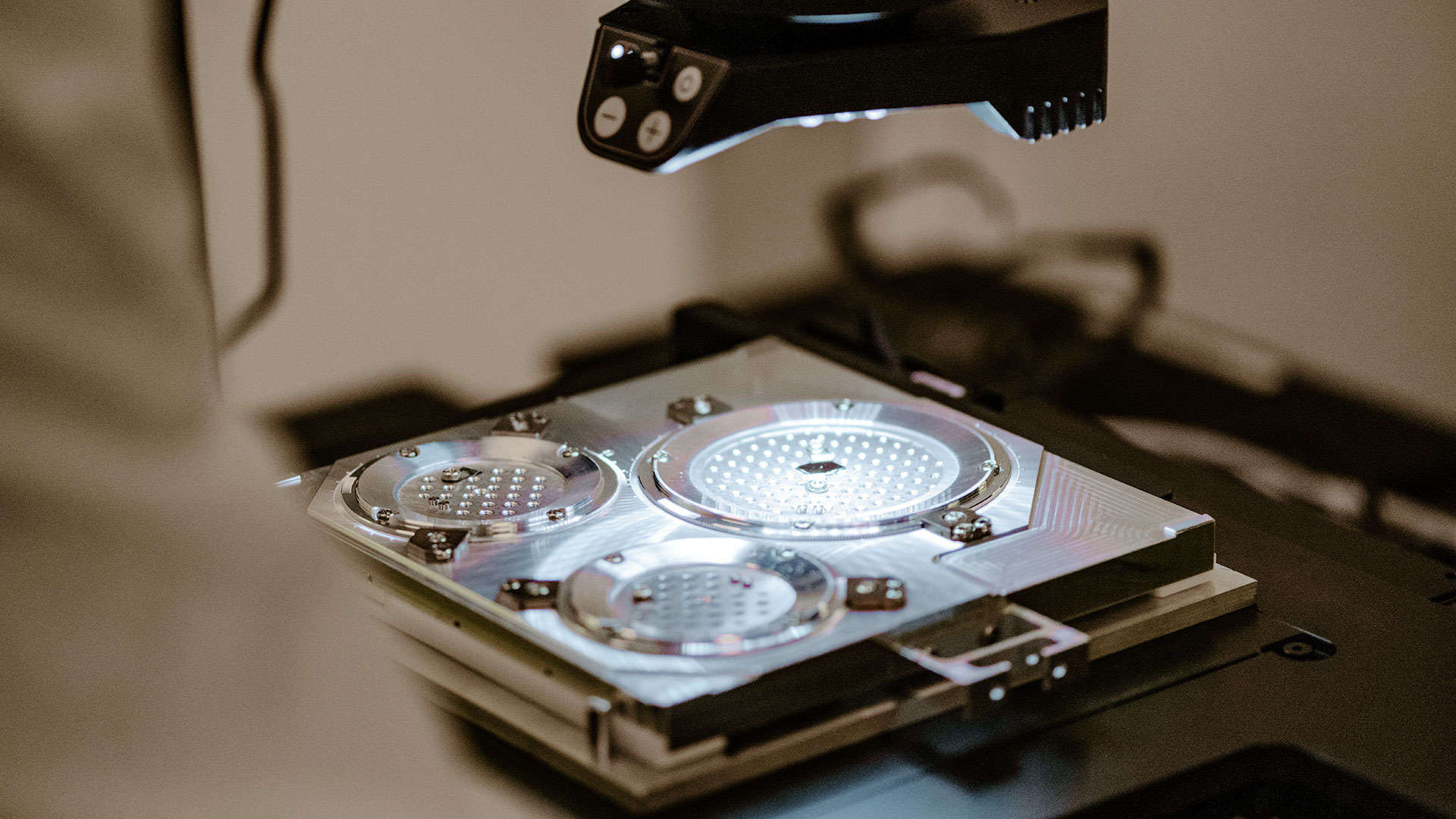
The Intelligent Codesign Cloud Lab for Non-Equilibrium and Low-Dimensional Materials (ICoN-PCL) is a Purdue-led node of the NSF programmable cloud lab network. It joins 2D-material synthesis, nanofabrication, additive manufacturing and extreme-condition testing to a shared data, digital-twin, and AI platform, all reachable from a browser.
New materials arrive far faster than we can use them.
2D transition metal dichalcogenides (TMDs) and MXenes have been in the literature for over a decade. Neither has made it into advanced devices or structural alloys at scale. Accelerated discovery of new materials has not been matched by an increase in the rate of insertion into devices and products.
Point solutions, not pipelines
Self-driving labs have proven the concept, but each one covers a single step. Nothing spans synthesis through fabrication, manufacturing, and qualification, so codesign never happens.
A design space too large to brute force
A single transistor gate stack has more than ten million plausible process conditions once you count material combinations, thicknesses, pressures, deposition rates, and temperatures. High-throughput search alone will not find the answer.
Access one instrument at a time
Even where facilities are open to outside users, access is granted one instrument at a time and largely in person. Nothing composes those steps into a single workflow, capability is duplicated across campuses, and researchers without a local cleanroom are left out.
Two problems worth building a Programmable Cloud Lab around
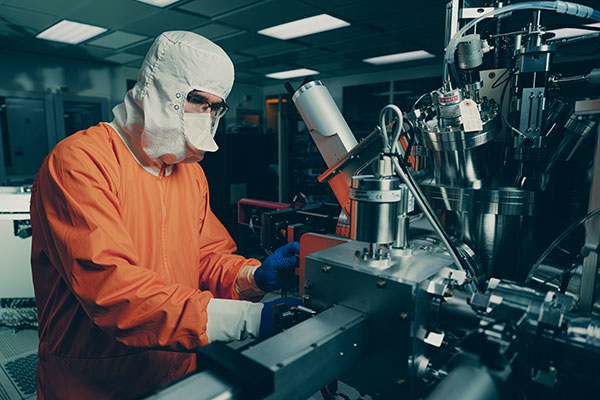
Area 1: 2D materials for electronic devices
TMDs are the leading candidate channel material for transistors scaled below 5 nm, and MXenes carry current densities on the order of 10⁸ A/cm². In both cases performance is decided at the interface rather than by any bulk property, and the interfaces are exactly what today's design rules cannot describe.
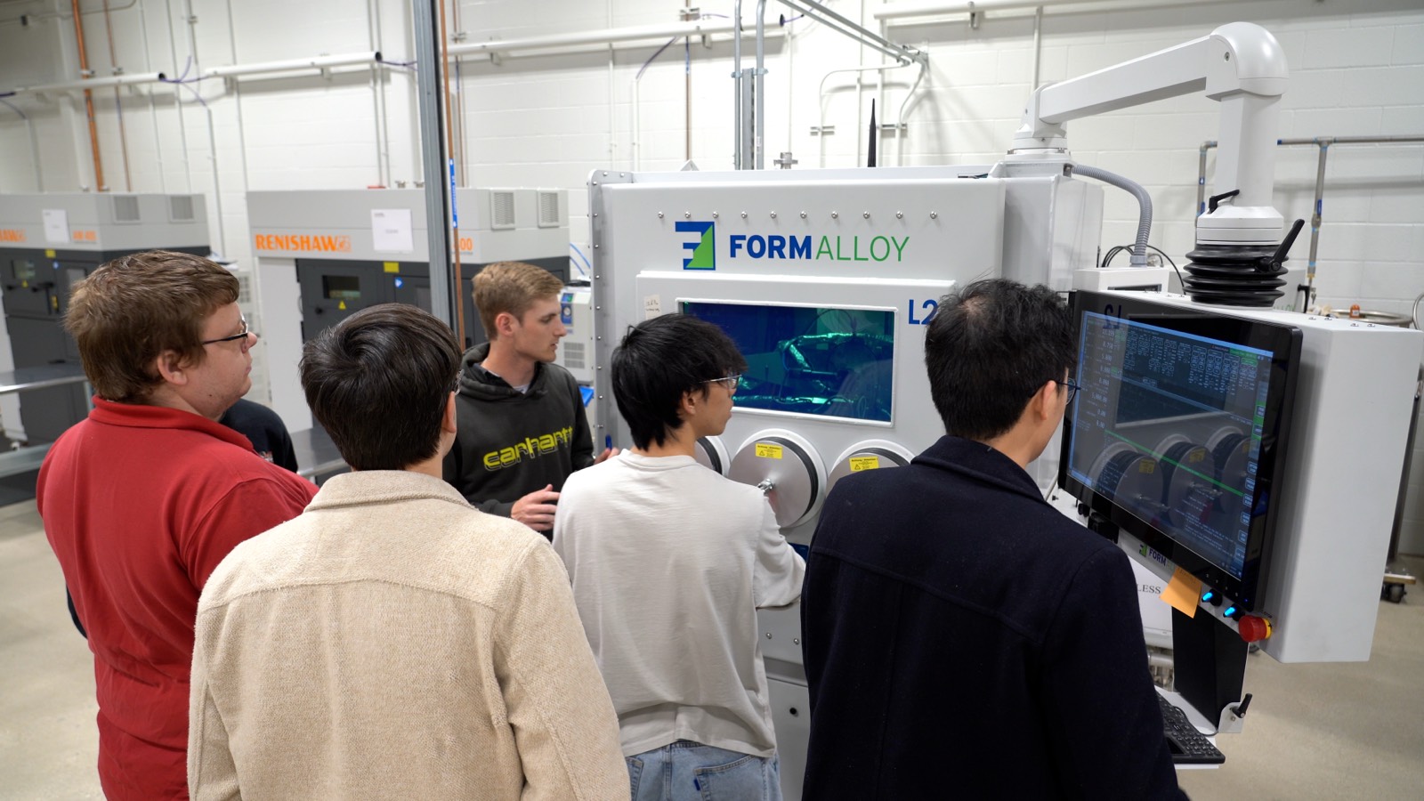
Area 2: advanced manufacturing of alloys with nanoparticle dispersions
NASA's GRX-810 showed what nanoscale oxide dispersions plus laser powder bed fusion can do: roughly twice the strength and a thousandfold gain in creep resistance. The equivalent using 2D dispersions has not materialized, because conventional processing destroys them.
Programmable physical assets, programmable digital assets
One continuum of instruments you can program remotely, and one platform of digital assets that plans, predicts, and records what those instruments do.

Physical assets
Synthesis, fabrication, manufacturing, characterization, and testing, arranged as one pipeline rather than five separate facilities. A sample can move from precursor to tested part without leaving the system, and each step accepts instructions from a remote user instead of requiring one in the room.

Digital assets
Simulations, FAIR and secure data, digital twins, and education. These are what make the instruments usable at a distance: the twin predicts what an experiment will do before it runs, the data comes back in a form other people can query, and the training material is tied to the equipment it describes.
Six service areas, one continuum
The test bed is funded and being built. Nothing here is accepting remote users yet, so this page describes what ICoN-PCL will offer, and what you can already use today.
Synthesis
2D material growth including TMDs, and MXene synthesis from MAX precursors through etching, dispersion, and drying.
Nanofabrication
Cluster deposition with in-situ characterization: ALD dielectrics, gate metals, MXene layers and XPS inspection without breaking vacuum.
Manufacturing
Laser-based additive manufacturing of metal-MXene feedstocks, wire EDM sectioning, autonomous heat treatment, CNC machining, and cold spray.
Characterization & testing
Diffraction, residual stress, and topography, plus mechanical testing to 2,200 °C, aqueous corrosion, and high-temperature oxidation.
Data & AI
FAIR metadata at the source, predictive digital twins with uncertainty, and the ICoN Research Assistant guiding planning and execution.
Training & education
Self-guided modules on nanoHUB, small-group consultations, and digital-twin environments to rehearse an experiment before it runs.
While we instrument our physical assets, learn about digital ones.
ICoN-PCL builds on infrastructure that is already open. These resources exist today, are free to academic users, and are the same platforms the testbed will run on.
nanoHUB
More than 900 research-grade simulation tools in a browser, used by 250,000+ people, backed by a FAIR repository of more than 1.5 million entries and 8,000+ educational resources. No install, no allocation request.
AURA research assistant
nanoHUB's agentic research assistant plans and runs simulations across 240+ tools and queries the FAIR results database on your behalf. The ICoN Research Assistant is being built on it.
Birck and MMRL today
Both facilities already serve external users through Purdue's recharge system: Birck supports over 600 users a year and onboarded 243 new ones in 2025, and MMRL runs about 20 projects a month, 30% of them for outside users.
Built on facilities that already run at national scale
Who ICoN-PCL is for
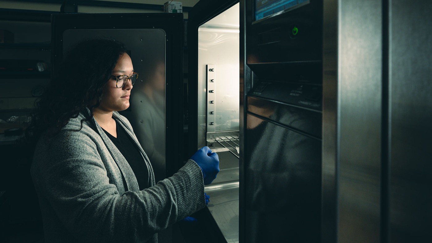
Eight user communities shaped the design, from aerospace and hypersonics to nuclear and fusion energy, electronics and semiconductors, transportation, critical materials, quantum, national laboratories, and educators at institutions without their own cleanroom.
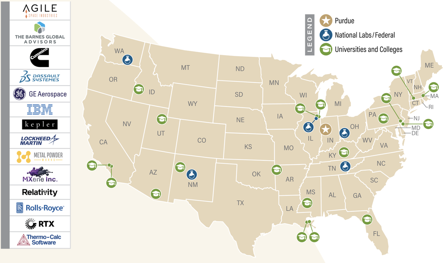
The partner network already spans 20 universities, 15 industry partners, and seven groups across five national laboratories, working with the team on experimental, data, and AI workflows.
Where it will run
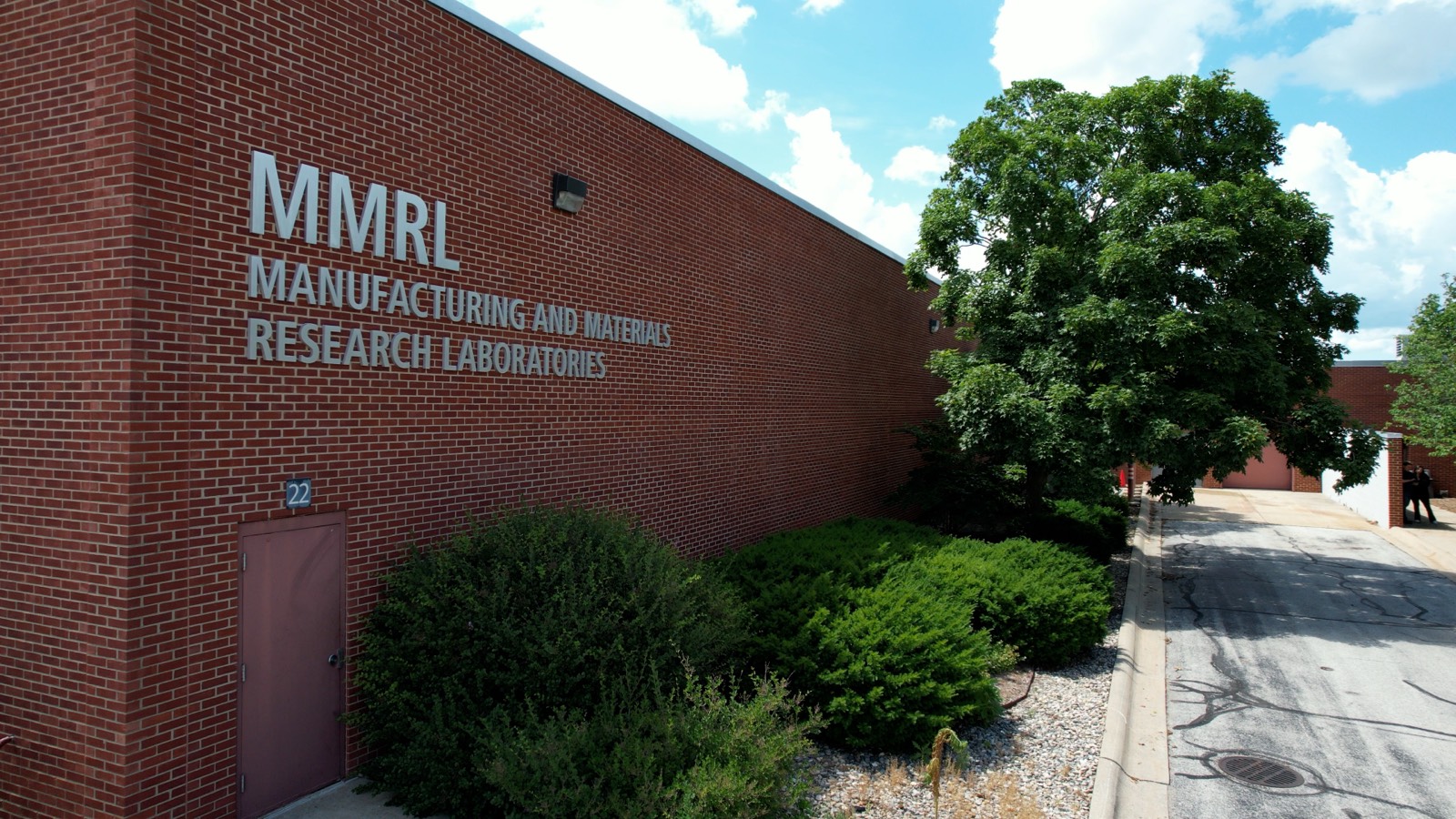
Physical assets are housed at the Birck Nanotechnology Center and the Manufacturing and Materials Research Laboratories on Purdue's West Lafayette campus. nanoHUB is the access point for remote users and the home of the digital assets.
Interoperability with other programmable cloud labs and self-driving labs is a design requirement, not an afterthought.
Tell us what you would run.
Services are not open yet. If you want to hear when a capability comes online, or you want to talk about partnering, contributing equipment or software, or bringing your community in, get in touch.
Following the project
ICoN-PCL is funded and in its start-up phase. This portal will grow into the front door for onboarding, service discovery and research planning as capability comes online. In the meantime, the About page explains the plan, the FAQ answers the questions we hear most, and Support tells you how to reach the team.