An instrument for material-process codesign.
The Intelligent Codesign Cloud Lab for Non-Equilibrium and Low-Dimensional Materials (ICoN-PCL) is a Purdue-led NSF Programmable Cloud Lab test bed. It integrates programmable laboratories spanning synthesis through fabrication with a data and AI platform for designing, optimizing, and executing research workflows.
What we are building: a set of programmable laboratories, from synthesis through fabrication, integrated with a data and AI platform for designing, optimizing, and running research workflows.
The bet: that opening these resources to far more people makes material–fabrication codesign possible for the first time, and shortens the path from a new material to a validated device or alloy. Testing a newly synthesized MXene as a strengthening dispersion in a metallic alloy takes months or years today. It should take days.
What the testbed is being built to answer
Area 1: 2D materials for electronic devices
TSMC, Intel, Samsung and imec all point to 2D materials as a leading path for future logic devices. The reason is a thickness problem: silicon's carrier transport degrades sharply once the channel body thins below a few nanometers, while TMDs stay semiconducting and keep useful transport down to a single monolayer under 1 nm thick. That makes them the leading candidate channel material at the 5 nm node and below. Van der Waals 2D–2D contacts help on the injection side, reducing the Fermi-level pinning and metal-induced gap states that dominate conventional metal–semiconductor junctions. Hole injection is the harder half: low-resistance p-type contacts to TMDs are not solved, and that is one of the interface problems this test bed exists to attack.
MXenes are candidates for ultra-scaled, highly conductive source and drain materials, carrying current densities on the order of 10⁸ A/cm², which is well above what electromigration permits in copper interconnects. TMDs are also under study for advanced interconnects and non-volatile memories.
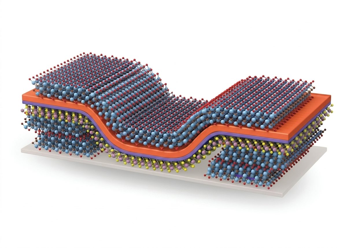
The central obstacle is interface control. Because these materials are two-dimensional, interfaces dominate performance and ultimately determine device properties, interfacial defects are not well controlled, and the design space across materials, stacks and processing runs to millions of configurations. Direct bottom-up growth of MXenes and their wafer-level deposition must both be solved before 2D device manufacturing is realistic.
Searching a space this large is not a throughput problem alone; it is a planning problem. Predictive twins and agent-driven design are what make the search tractable, and we will publish experiments-per-staff-hour as the test bed comes online.
Area 2: advanced manufacturing of alloys with nanoparticle dispersions
Advanced structural alloys today rely on precipitating thermodynamically favourable second phases or mixing in block ceramics. Oxide dispersion strengthening is the reference case: NASA's GRX-810 disperses ~20 nm yttria particles through a NiCoCr-based alloy and reports roughly twice the tensile strength and over a thousandfold longer creep life than comparable superalloys. The same approach using 2D dispersions has not been achieved, because processing conditions destroy them.
The approach here is to wrap metal powder particles in MXene before melting, so few-atom-thick metal carbide layers survive into the finished part and sit at the grain boundaries. What remains unclear is the mechanism governing strengthening, stability, and degradation, how much control manufacturing can exert over dispersion and phase evolution, and which of a vast space of low-dimensional additives is worth using at all.
ICoN-PCL is assembling an autonomous workflow spanning additive manufacturing, sample preparation, heat treatment, room- and high-temperature mechanical testing, aqueous corrosion testing, and surface integrity measurement, so base alloy, low-dimensional phase and microstructure can be co-optimized rather than chosen one at a time.
Where the capability lives
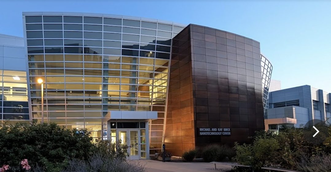
Birck Nanotechnology Center
186,000 sq ft of shared cleanroom, laboratory, and office space, including a 25,000 sq ft class 1/10/100 cleanroom carrying 220+ tools for patterning, deposition, etching, thermal annealing, and packaging, and 33,000 sq ft of characterization space.
Open since 2005. Eighteen engineers and six scientists support more than 600 users a year, and 243 new users were onboarded in 2025. A $70M+ upgrade program running 2023 to 2027 is bringing the facility to 8-inch wafer compatibility.
MMRL
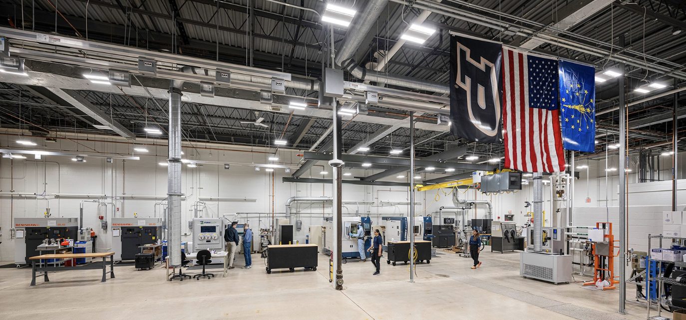
30,000 sq ft of additive manufacturing, characterization and testing capability for metallic and composite materials, opened in 2022 on more than $10M of Purdue investment.
Three technical, two administrative and four research staff run roughly 20 projects a month, 30% of them for users outside MMRL: government laboratories, nuclear startups, materials manufacturers, and aerospace companies.
nanoHUB
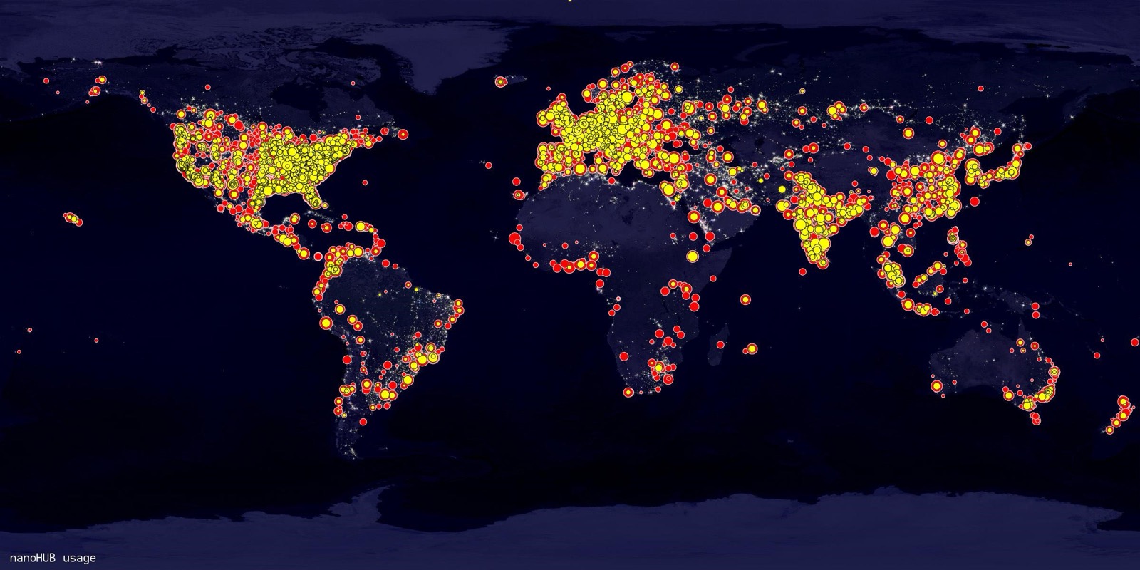
Open since 2002 and built on more than $70M of federal investment. More than 900 simulation tools, 250,000+ users, a FAIR repository of over 1.5 million entries and 8,000+ educational resources. It reaches 937 US universities, 799 of them non-R1, and every one of the top 50. It is the access point for ICoN-PCL's remote users and digital assets.
From idea to executed experiment
-
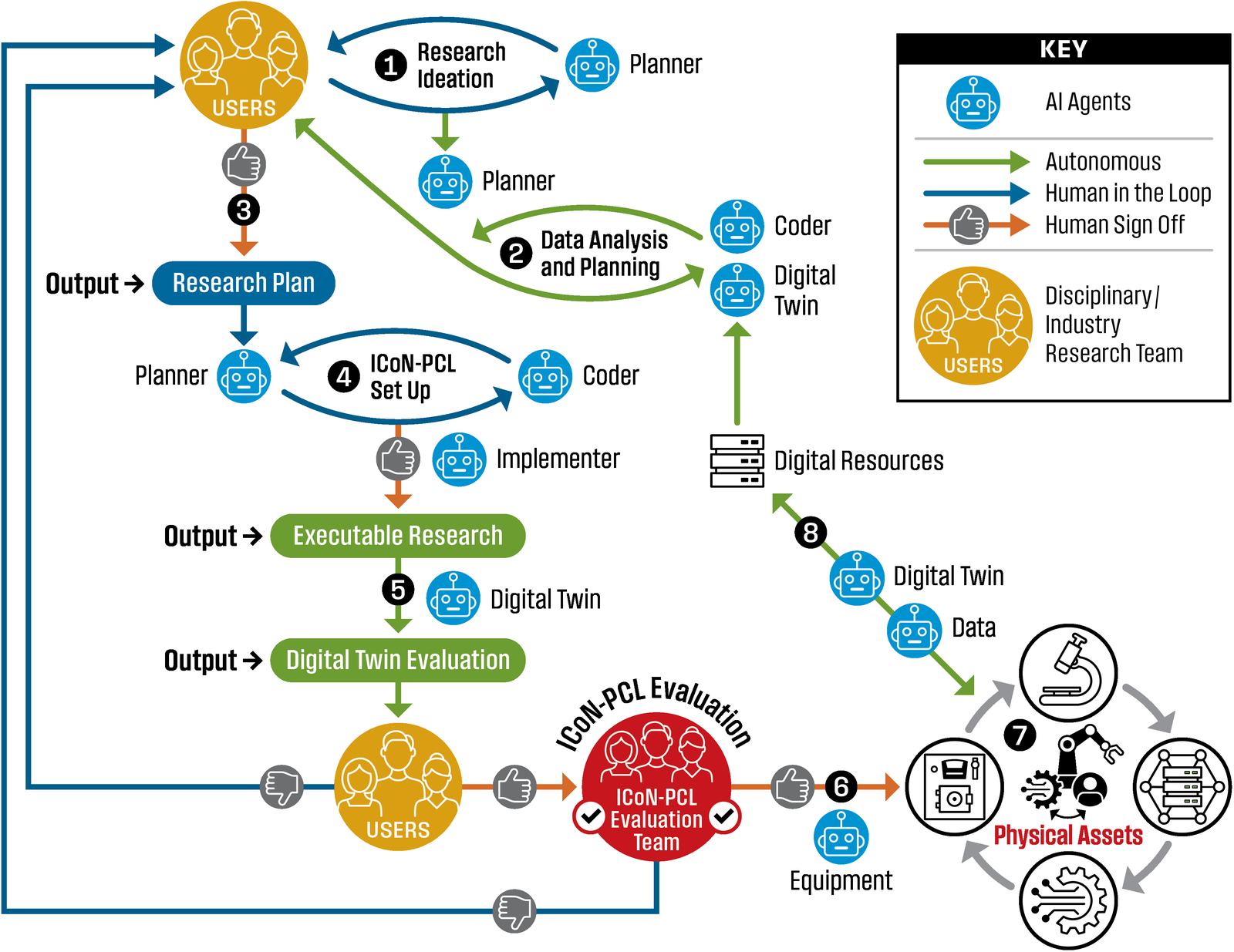
Ideation and planning
You describe the question. The ICoN Research Assistant's Planner Agent gathers and analyzes prior data, then drafts a research plan with you.
-
Implementation
Once you sign off, Implementer and Digital Twin agents translate the plan into a detailed execution procedure in a laboratory domain-specific language.
-
Evaluation
Equipment and digital-twin agents predict the most likely outcome, and check safety and feasibility. That report goes to you and to the ICoN-PCL Evaluation Team.
-
Execution
Approved projects are scheduled against real instrument availability and run on the physical assets, with every input, output and log indexed under a unique sample identifier.
FAIR by construction, not by cleanup
Metadata and provenance
All experimental data and metadata are captured at the source, converted to AI-ready formats and linked to an extensible metadata framework. The ICoN-PCL Metadata Core draws on Dublin Core terms and domain schemes including Sandia's eOS and MatCore, stays compatible with W3C DCAT, and packages data, software, and provenance with RO-Crate. Persistent identifiers such as DOIs and ORCIDs run through the framework so citation and credit are automatic.
Cyber-physical passports
Purdue-developed and patented cyber-physical passports provide certified, immutable records of fabrication entities, processes, artifacts, and products. A fabricated part's passport carries its equipment time-series data, layouts, and resulting material properties together.
Access control
Users register with an institutional email and agree to an end-user license agreement, with separate agreements for educational, research, and commercial use. Activity is monitored for compliance, and deviations trigger human follow-up.
Nothing runs unreviewed
Before a physical experiment, digital twins assess every step of the proposed workflow for outcome and safety, and a laboratory staff member reviews both the tasks and the digital-twin analysis and signs off. First-time user material covers fundamentals, equipment operation, and laboratory safety, and the Evaluation Team monitors safety culture alongside lab staff.
Proven at scale
This is not new ground for the team: nanoHUB already hosts commercial tools from Thermo-Calc, Cadence, Synopsys, and Siemens, each with distinct access requirements, alongside fully open tools.
Beyond the award period
ICoN-PCL is designed to outlive its initial funding. nanoHUB has operated continuously since 2002 with and without NSF support; Birck and MMRL are sustained by a mix of public and private stakeholders. Continued operation is planned through cost sharing across those three facilities plus a fee structure that keeps access subsidized for academic and non-R1 users while charging industrial and high-intensity users at standard rates.